5901 Botham Jean Blvd, Dallas, TX 75215
What is Cleanroom Equipment Recycling in Semiconductor Fabs?
August 1, 2025In the precise world of semiconductor manufacturing, every particle is significant. Cleanroom equipment recycling is a growing sustainability practice where used machinery, components, and materials from semiconductor fabrication facilities are carefully recovered, restored, and reintroduced into production cycles.
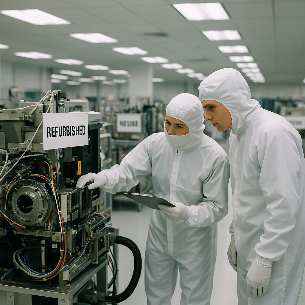
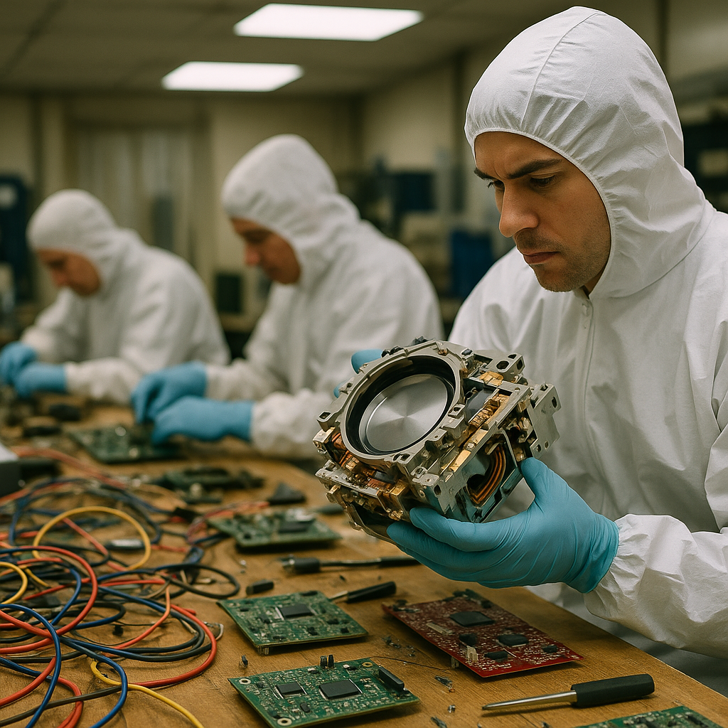
The process involves specialized techniques to refurbish equipment that once operated in highly controlled environments. Technicians meticulously clean, test, and recalibrate items ranging from wafer handling systems to air filtration units. This ensures the recycled equipment meets the stringent standards required for semiconductor production.
Resource conservation is central to this practice. By extending the lifespan of specialized cleanroom equipment, semiconductor manufacturers significantly reduce their dependence on virgin materials. This approach not only preserves valuable resources but also offers substantial cost benefits by minimizing the need for new purchases and lowering waste disposal expenses.
What Are the Benefits of Recycling Semiconductor Fab Equipment?

Recycling semiconductor fabrication equipment offers substantial benefits for both manufacturers and the environment. Companies in this sector face growing pressure to reduce waste while maintaining profitability, and responsible recycling practices address both challenges effectively.
Resource Conservation
The semiconductor manufacturing process requires substantial raw materials. Recycling fab equipment minimizes the need for extracting new materials by repurposing components that would otherwise require new production.
When semiconductor companies recycle silicon wafers, they lessen reliance on newly mined silicon. This conservation method extends the lifespan of existing materials and reduces resource depletion across the supply chain.
Advanced reclamation techniques have changed how manufacturers view used wafers. Through chemical etching, mechanical polishing, and thermal treatments, facilities can restore the surface integrity of previously discarded components.
Significant Cost Savings
Financial benefits are a primary driver for fab equipment recycling programs. The high costs of acquiring new components and materials can be significantly offset through recycling.
Companies that implement recycling initiatives save on reduced raw material purchases and minimize expenses associated with waste disposal and regulatory compliance.
Reclaiming valuable materials like gold and other precious metals from discarded wafers further enhances cost efficiency, offsetting production expenses and improving economic viability throughout manufacturing cycles.
Environmental Impact Reduction
Traditionally, semiconductor manufacturing has generated considerable waste and emissions. Recycling programs directly address these environmental concerns.
By diverting fab equipment from landfills, companies decrease waste volume and associated land use impacts. Recycling also reduces greenhouse gas emissions by lowering the need for energy-intensive production of new components.
Water conservation is another key benefit. Closed-loop water systems in recycling facilities recapture and purify process water, preventing wastewater discharge and reducing overall consumption.
Circular Economy Promotion
Recycling semiconductor equipment supports a circular economic model, where materials maintain their value through continuous reuse, transforming the traditional linear “take-make-dispose” paradigm.
Incorporating recycled components into production builds resilience within supply chains, reducing vulnerability to raw material shortages and price fluctuations.
The industry’s shift toward circular practices fosters innovation, leading to the development of new recycling technologies and processes that enhance efficiency and create new business opportunities.
The adoption of these recycling practices aligns with increasing regulatory requirements and corporate sustainability goals. Many semiconductor manufacturers have already embraced comprehensive recycling programs that significantly reduce their environmental footprint while improving operational efficiency.
What Challenges Exist in Recycling Semiconductor Fab Equipment?

The semiconductor industry faces significant hurdles in recycling fabrication equipment. These challenges extend beyond logistics, necessitating innovative solutions for environmental sustainability and economic viability.
Recycling semiconductor fab equipment requires specialized expertise due to the complex nature of its components. Unlike consumer electronics recycling, fab equipment involves precision instruments calibrated for cleanroom environments. Technicians with extensive knowledge are needed to dismantle these systems without damaging valuable components.
The technical complexity manifests in various ways. Fab tools contain multiple materials that must be separated—from rare earth metals and specialized alloys to hazardous chemicals used in etching and deposition processes. Each material requires different handling protocols and recycling pathways. Additionally, large-scale recycling infrastructure for some components is still lacking.
Quality Assurance Hurdles
A major challenge is ensuring that recycled equipment meets the stringent standards of semiconductor manufacturing, which leaves no room for error. Even microscopic contaminants can render products unusable.
Reclaimed equipment must undergo rigorous testing to ensure it meets specifications. This verification process adds significant costs to recycling operations. Testing protocols must confirm not only basic functionality but also performance metrics like:
- Surface uniformity and cleanliness
- Vacuum integrity for systems needing ultra-high vacuum conditions
- Precise calibration of sensors and control systems
- Complete removal of process chemicals and contaminants
Manufacturers often hesitate to use recycled equipment for producing cutting-edge chips with nanometer-scale features. Equipment failure or quality issues could lead to costly scrapped wafers and production downtime.
Economic Constraints
The economics of fab equipment recycling add another layer of complexity. Specialized recycling facilities require substantial investment. Industry research indicates that the cost of recycling certain types of semiconductor equipment can reach $147 per ton, compared to $28 per ton for conventional landfill disposal.
The initial investment in a fab can exceed $5 billion, with daily operational costs over $3 million. Given such high stakes, manufacturers need evidence that recycled equipment won’t compromise production quality or reliability.
Water reclamation systems highlight this challenge. While semiconductor facilities can achieve water recovery rates up to 60% through recycling, these systems require significant space, capital, and maintenance. Thus, many facilities opt to treat and discharge wastewater instead of investing in comprehensive recycling infrastructure.
Technical Solutions Emerging
Despite these obstacles, the industry is developing solutions. Equipment vendors now offer refurbishment services to upgrade used equipment to current specifications. These programs involve complete disassembly, thorough cleaning, component replacement, and detailed testing.
Innovations in validation are also emerging. Advanced testing protocols can verify the performance of recycled components with greater precision, reducing the risks of using reclaimed equipment.
Some manufacturers have shifted to targeted recycling approaches instead of comprehensive end-of-pipe solutions. By segregating specific waste streams from processes like etching, rinsing, and die cutting, they can implement more effective recycling for each unique waste type.
The semiconductor industry continues to balance technical challenges with sustainability goals. Through collaboration between manufacturers, equipment suppliers, and recycling specialists, the sector is gradually developing more effective approaches to equipment recycling, turning what was once waste into valuable resources for manufacturing.
While perfect solutions remain elusive, each improvement in recycling technology brings the industry closer to sustainable operations without compromising the standards that modern semiconductor manufacturing demands.
What is the Future of Cleanroom Equipment Recycling in Semiconductor Fabs?

The outlook for cleanroom equipment recycling in semiconductor fabs is promising. This growth is fueled by technological advancements and a heightened focus on environmental sustainability within the industry. As global demand for electronic devices continues to increase, semiconductor manufacturers are adopting more sustainable practices to minimize their environmental impact while maintaining production efficiency.
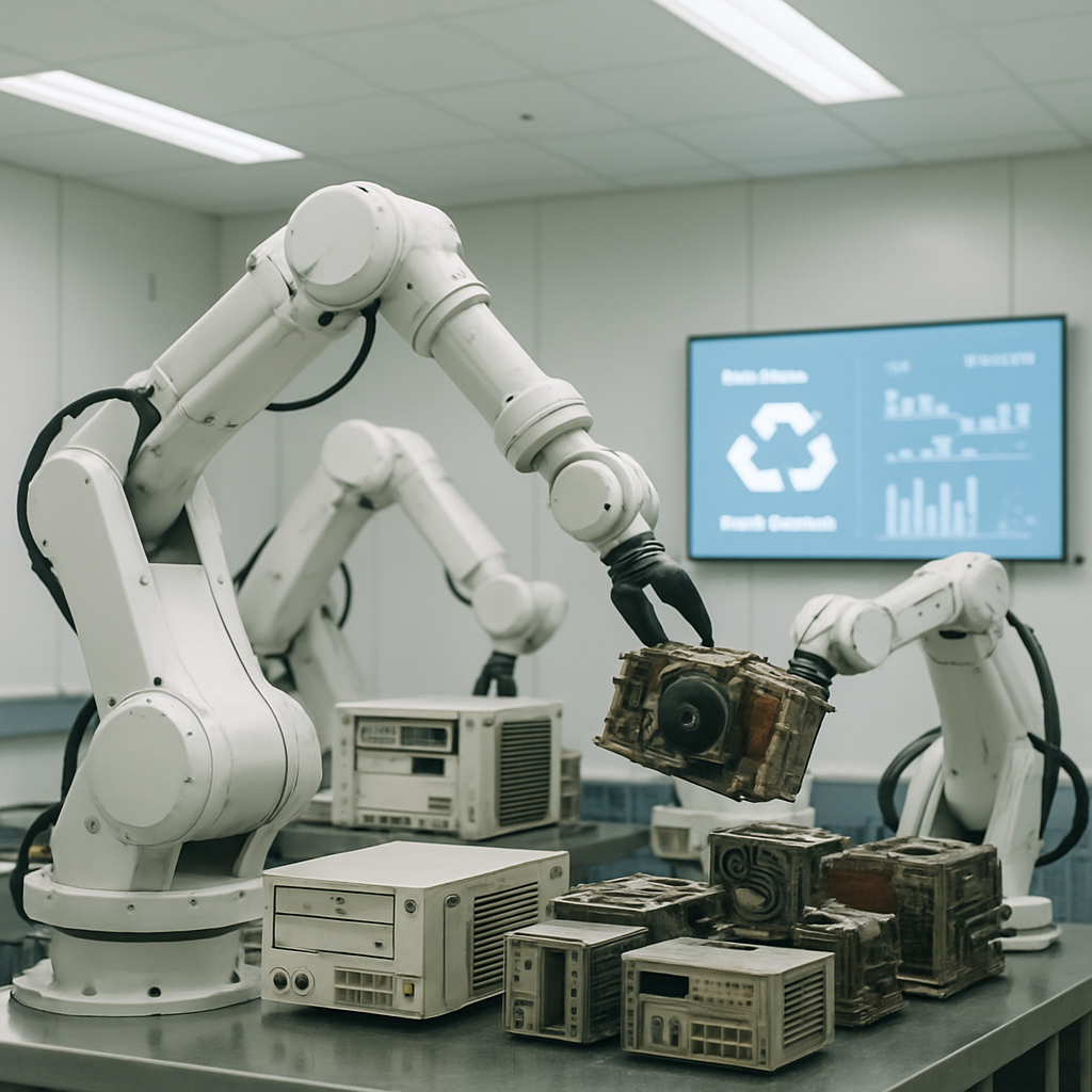
Recycling technologies are quickly evolving to address the specific needs of semiconductor fabrication facilities. Innovations in automation, data monitoring solutions, and energy-efficient technologies enhance the recycling process’s effectiveness. This progress allows manufacturers to recover valuable materials from equipment while upholding the stringent cleanliness standards essential in semiconductor production.
For inquiries about specialized recycling solutions for your semiconductor cleanroom equipment, contact Okon Recycling at 214-717-4083.
